
prepare a Pcb production for testing
Testing is a crucial phase in PCB production, as it ensures the final product functions as intended and meets the desired performance standards. Proper testing not only identifies potential flaws or defects in the PCB design but also helps verify the electrical integrity, signal quality, and overall reliability of the assembled board. Preparing a PCB production for testing involves a series of important steps that include design considerations, pre-production checks, and selecting the appropriate testing methods. In this article, we will explore how to prepare a PCB production for testing to ensure that the testing phase is efficient and effective.
The preparation for PCB testing starts well before the actual production phase, with careful consideration of the design. Design for Testability (DFT) is a key principle in PCB design that ensures the PCB can be easily and thoroughly tested after production. DFT includes designing the board so that test points are accessible, critical components can be measured for functionality, and electrical pathways are easily traceable. Test points are pads or pins specifically designed on the PCB for testing probes or measurement instruments to connect during the testing phase.
Moreover, during the design phase, PCB designers should also plan for the integration of built-in self-test (BIST) features, which allow the board to perform certain diagnostic checks on its own. This can be particularly useful for complex or high-speed circuits, where manual testing may be difficult or time-consuming. By addressing these design considerations, PCB production becomes much easier to test, resulting in faster identification and resolution of potential issues.
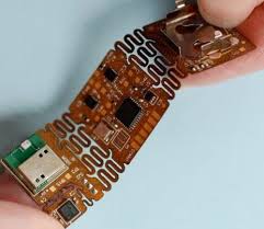
How do you prepare a Pcb production for testing?
Before moving into full-scale pcb production, several pre-production checks should be performed to ensure that the PCB design is ready for testing. These checks involve verifying that the design follows manufacturing specifications and standards and that it meets the requirements for testability. Design Rule Checks (DRC) and Electrical Rule Checks (ERC) are commonly used to identify any design errors that could complicate the testing process.
In addition to these checks, a Design for Manufacturability (DFM) review should be conducted to ensure that the design is feasible and that the components selected are appropriate for the intended testing methods. For example, if automated testing is planned, the design should include sufficient access points for test probes, as well as clearly marked pads and vias. Furthermore, before production begins, the board design should be reviewed to confirm that it will meet the necessary compliance and performance standards, ensuring that the testing process will yield accurate results.
Once the appropriate testing methods are selected, a detailed test plan should be created. This plan should outline the testing steps, test equipment, test points, and expected results. The test plan should also specify any requirements for environmental conditions, such as temperature and humidity, that might affect the performance of the PCB during testing. Additionally, the test plan should include a timeline and procedures for troubleshooting any issues that arise during the testing phase.
Having a clear test plan ensures that all aspects of the PCB are tested thoroughly, and it provides a systematic approach for identifying and addressing issues. A well-prepared test plan helps streamline the testing process, saving time and resources while ensuring that the final product meets performance and quality standards.